- 您现在的位置:买卖IC网 > Sheet目录1992 > CY28551LFXC-3T (Silicon Laboratories Inc)IC CLOCK INTEL/AMD SIS VIA 56QFN
CY28551-3
......................Document #: 001-05677 Rev. *D Page 3 of 28
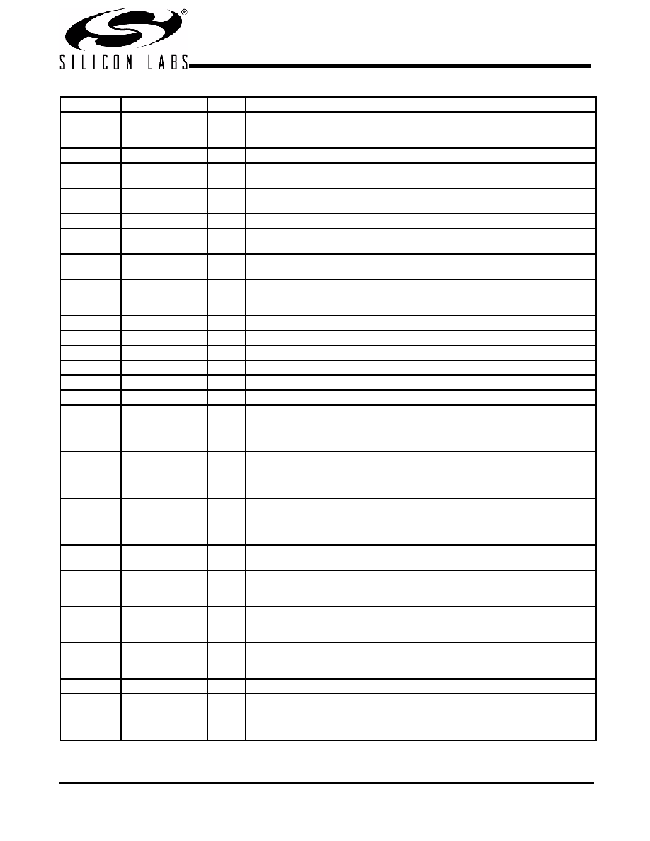
31
**DOC2
I, PD
Dynamic Over Clocking pin
0 = normal, 1 = Frequency will be changed depend on DOC register. Internal 150k
pull-down.
32
VSSCPU
GND
Ground for outputs.
33
CPUC1
O, DIF Complement Differential CPU clock output.
Intel type SR output buffer.
34
CPUT1
O, DIF True Differential CPU clock output.
Intel type SR output buffer.
35
VDDCPU
PWR
3.3V power supply for outputs.
36
CPUC0
O, DIF Complement Differential CPU clock output.
Intel type SR output buffer.
37
CPUT0
O, DIF True Differential CPU clock output.
Intel type SR output buffer.
38
VTT_PWRGD#/PD
I
3.3V LVTTL input. This pin is a level-sensitive strobe used to latch the HW strapping
pin inputs. After asserting VTT_PWRGD# (active LOW), this pin becomes a
real-time input for asserting power-down (active HIGH)
39
SDATA
I/O
SMBus compatible SDATA
40
SCLK
I
SMBus compatible SCLOCK.
41
VDDREF
PWR
3.3V power supply for outputs.
42
XOUT
O
14.318-MHz Crystal Output
43
XIN
I
14.318-MHz Crystal Input
44
VSSREF
GND
Ground for outputs.
45
**MODE/REF2
I/O, SE,
PD
3.3V-tolerant input for selecting output/14.318-MHz REF clock output. Internal 150k
pull-down
0 = Desktop, 1 = Notebook
Intel Type-5 output buffer
46
**FSC/REF1
I/O,PD,
SE
3.3V-tolerant input for CPU frequency selection/14.318-MHz REF clock output.
Internal 150k pull-down
Intel Type-5 output buffer
Refer to DC Electrical Specifications table for Vil_FS and Vih_FS specifications.
47
**FSD/REF0
I/O,PD,
SE
3.3V-tolerant input for CPU frequency selection/14.318-MHz REF clock output.
Internal 150k pull-down
Intel Type-5 output buffer
Refer to DC Electrical Specifications table for Vil_FS and Vih_FS specifications.
48
RESET_I#/SRESE
T#
I/O, OD 3.3V-tolerant input for reset all of registers to default setting.
3.3V LVTTL output for watchdog reset signal
49
**DOC1
I, PD
Dynamic Over Clocking pin
0 = normal, 1 = Frequency will be changed depend on DOC register. Internal 150k
pull-down
50
**CLKREQ#B/PCI0 I/O,SE,
PD
3.3V tolerant LVTTL input for Output enable of PCIEX 4,5 via register
selection/33-MHz clock output. Internal 150k pull-down
Intel Type-3A output buffer
51
**CLKREQ#A/PCI1 I/O,SE,
PD
3.3V-tolerant LVTTL input for Output enable of PCIEX 6,7 via register
selection/33-MHz clock output. Internal 150K pull-down
Intel Type-3A output buffer
52
VSSPCI
GND
Ground for outputs.
53
**FSA/PCI2
I/O, PD 3.3V-tolerant input for CPU frequency selection/33-MHz clock output. Internal 150k
pull-down
Intel Type-3A output buffer
Refer to DC Electrical Specifications table for Vil_FS and Vih_FS specifications
Pin Description (continued)
Pin No.
Name
Type
Description
发布紧急采购,3分钟左右您将得到回复。
相关PDF资料
CY28551LFXC
IC CLOCK INTEL/AMD SIS VIA 64QFN
CY2SSTV855ZXI
IC CLOCK DIFFDRV PLL DDR 28TSSOP
CY2SSTV857ZXI-27
IC CLK DDR266/333BUF1:10 48TSSOP
CY2SSTV857ZXI-32
IC CLK DDR266/333BUF1:10 48TSSOP
CY505YC64DT
IC CLK CK505 BROADWATER 64TSSOP
CYW150OXC
IC CLOCK 440BX AGP 56SSOP
CYW173SXC
IC CLK GEN TAPE DRV 4CH 16SOIC
CYW305OXC
IC CLOCK W305 SOLANO 56SSOP
相关代理商/技术参数
CY28551LFXCT
功能描述:时钟发生器及支持产品 Universal System Clk Intel AMD SiS Via RoHS:否 制造商:Silicon Labs 类型:Clock Generators 最大输入频率:14.318 MHz 最大输出频率:166 MHz 输出端数量:16 占空比 - 最大:55 % 工作电源电压:3.3 V 工作电源电流:1 mA 最大工作温度:+ 85 C 安装风格:SMD/SMT 封装 / 箱体:QFN-56
CY2862-000
制造商:TE Connectivity 功能描述:82A0111-4-9-G110
CY2863-000
制造商:TE Connectivity 功能描述:82A0111-8-9-G110 - Bulk
CY28800
制造商:CYPRESS 制造商全称:Cypress Semiconductor 功能描述:100-MHz Differential Buffer for PCI Express and SATA
CY28800OXC
功能描述:时钟缓冲器 PCI Express & Sata Diff Buffer 100MHz RoHS:否 制造商:Texas Instruments 输出端数量:5 最大输入频率:40 MHz 传播延迟(最大值): 电源电压-最大:3.45 V 电源电压-最小:2.375 V 最大功率耗散: 最大工作温度:+ 85 C 最小工作温度:- 40 C 封装 / 箱体:LLP-24 封装:Reel
CY28800OXCT
功能描述:时钟缓冲器 PCI Express & Sata Diff Buffer 100MHz RoHS:否 制造商:Texas Instruments 输出端数量:5 最大输入频率:40 MHz 传播延迟(最大值): 电源电压-最大:3.45 V 电源电压-最小:2.375 V 最大功率耗散: 最大工作温度:+ 85 C 最小工作温度:- 40 C 封装 / 箱体:LLP-24 封装:Reel
CY28800OXI
功能描述:时钟缓冲器 PCI Express & Sata Diff Buffer 100MHz RoHS:否 制造商:Texas Instruments 输出端数量:5 最大输入频率:40 MHz 传播延迟(最大值): 电源电压-最大:3.45 V 电源电压-最小:2.375 V 最大功率耗散: 最大工作温度:+ 85 C 最小工作温度:- 40 C 封装 / 箱体:LLP-24 封装:Reel
CY28800OXIT
功能描述:时钟缓冲器 PCI Express & Sata Diff Buffer 100MHz RoHS:否 制造商:Texas Instruments 输出端数量:5 最大输入频率:40 MHz 传播延迟(最大值): 电源电压-最大:3.45 V 电源电压-最小:2.375 V 最大功率耗散: 最大工作温度:+ 85 C 最小工作温度:- 40 C 封装 / 箱体:LLP-24 封装:Reel